


On September 27, Novus Semiconductors Co., Ltd. (Novusem) held an online product launch event. At the event, the company rolled out the first generation of NovuSiC® MOSFET (G1) and announced the mass production schedule of the second generation (G2). Dr. Gao Wei, Deputy General Manager of Novusem, delivered a keynote speech on product performance with the theme of "accumulating strength and continuing innovation." He also made a detailed introduction to the development milestones, design concept, and unique advantages of silicon carbide (SiC) MOSFETs. Wang Deqiang, an application engineer, demonstrated the application fields, application scenarios, and solutions around product application, reflecting Novusem's independent R&D strengths and its determination to compete in the automotive chip market.
Novusem, an Up-and-Coming Company Devoted to Blazing a New Trail
The world semiconductor industry started in the 1950s. Since the end of the 1970s, planar and trench power MOSFETs and IGBTs have come out one after another. As society's electrification level advances, power MOSFETs have evolved through process advancement, technology improvement, and material iteration. The breakthroughs of SiC in material preparation have greatly promoted the commercialization of SiC devices.
As a third-generation semiconductor material, SiC boasts outstanding physical properties like wide bandgap, high breakdown electric field strength, high thermal conductivity, and high electron saturation rate. This allows SiC power semiconductor devices to have remarkable advantages, such as high voltage resistance, high temperature resistance, fast switching speed, and low loss. With these advantages, SiC power devices can reduce circuit board space and lower system costs and energy loss, thus significantly improving power density and system efficiency. The Chinese domestic SiC MOSFET market relies mainly on imports due to its complex technology and process. With the rapidly increasing application and demand for new technologies in new energy vehicles, industrial power supplies, PV inverters, etc., there is a vast space for localization.
Established in December 2019, Novusem is the first high-tech enterprise in Sichuan Province dedicated to the design and development of wide-bandgap semiconductor SiC power devices. After more than 900 days of R&D, improvements, devotion, and strength accumulation, Novusem released NovuSiC® 1200V/75mΩ MOSFET G1 at this launch event, a follow-up to its self-developed SiC NovuSiC® EJBS™ (Enhanced Junction Barrier Schottky) diode series launched at the end of June 2022.
NovuSiC® 1200V/75mΩ MOSFET, A SiC Product with High Cost Performance and High Reliability
NovuSiC® 1200V/75mΩ MOSFET performs excellently in new energy vehicles, DC charging piles, PV systems, and other application scenarios, as it drastically reduces static and dynamic losses, increases system power density, and lowers the total system cost.
In the development of SiC MOSFETs, Novusem adopted a balanced and optimized approach to electrical performance, robustness, and reliability based on application scenarios. That is to say, Novusem improves the devices' robustness and long-term reliability by adopting measures such as using lower gate voltage drives, optimizing the gate oxide process and the electric field intensity of the gate oxide, and reducing the curvature effect of the junction terminal while taking into account the specific on-resistance (Ron,sp) and the electric field of the gate oxide.
In terms of electrical performance and robustness, NovuSiC® 1200V/75mΩ MOSFETs can achieve an on-resistance (Ron) of 75 mΩ and a Ron,sp of 4.6 when VGS is 20V, ranking among the best in the Chinese domestic market. When the withstand voltage is 1200V, the electric field strength of the gate oxide in the JFET region is far less than the conventional limit of 4.0 MV/cm, and the short-circuit withstand time is longer than 3μs under the condition where VDD is 800V. NovuSiC® 1200V/75mΩ MOSFET reduces the effective area of the JFET region while increasing the channel density, and optimizes the dynamic characteristics by reducing Cgd. Its gate charge (Qg) is comparable to that of international competitors, with a figure of merit (FOM) above the industry average, and it will reach the most advanced international technical standard from G2 (1Q '23), demonstrating Novusem's commitment to innovation and quality.
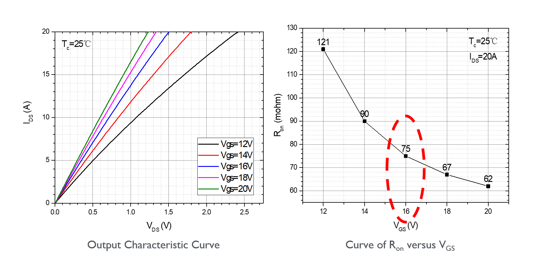
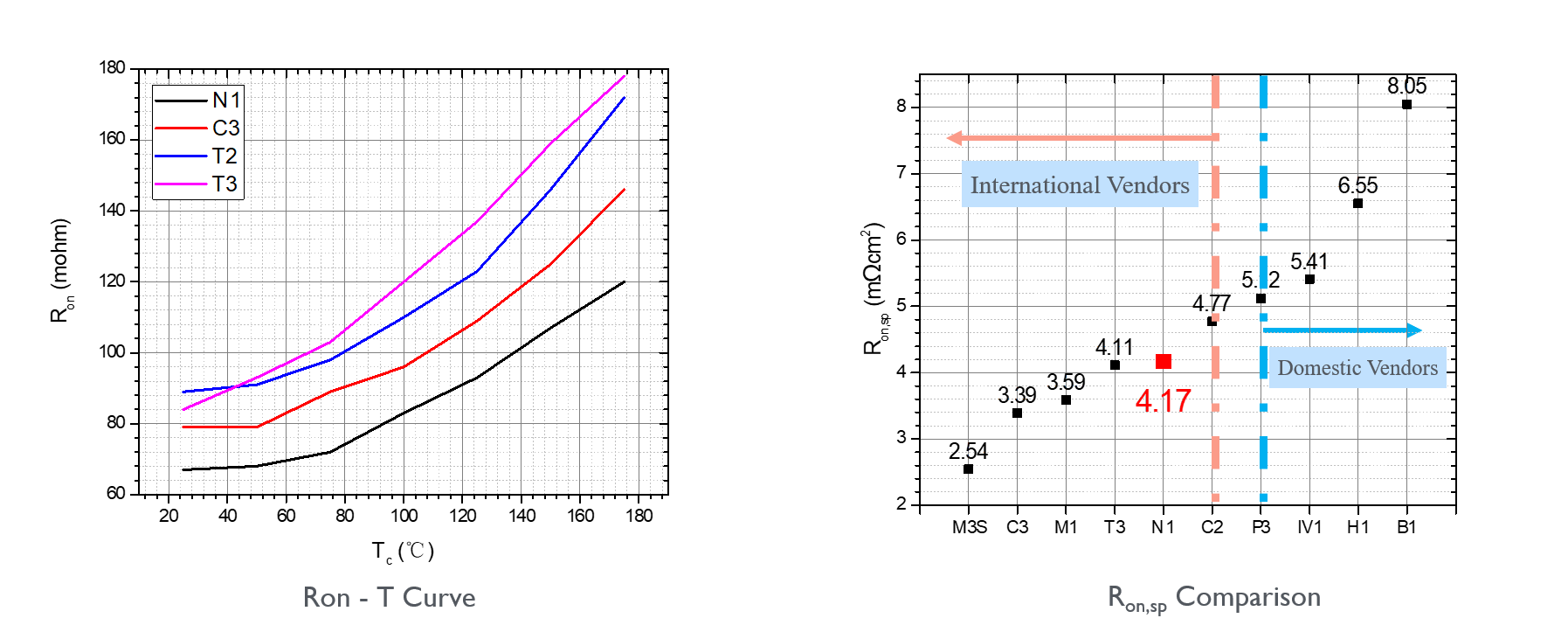
Figure 1: Conduction characteristics of NovuSiC® 1200V/75mΩ MOSFETs
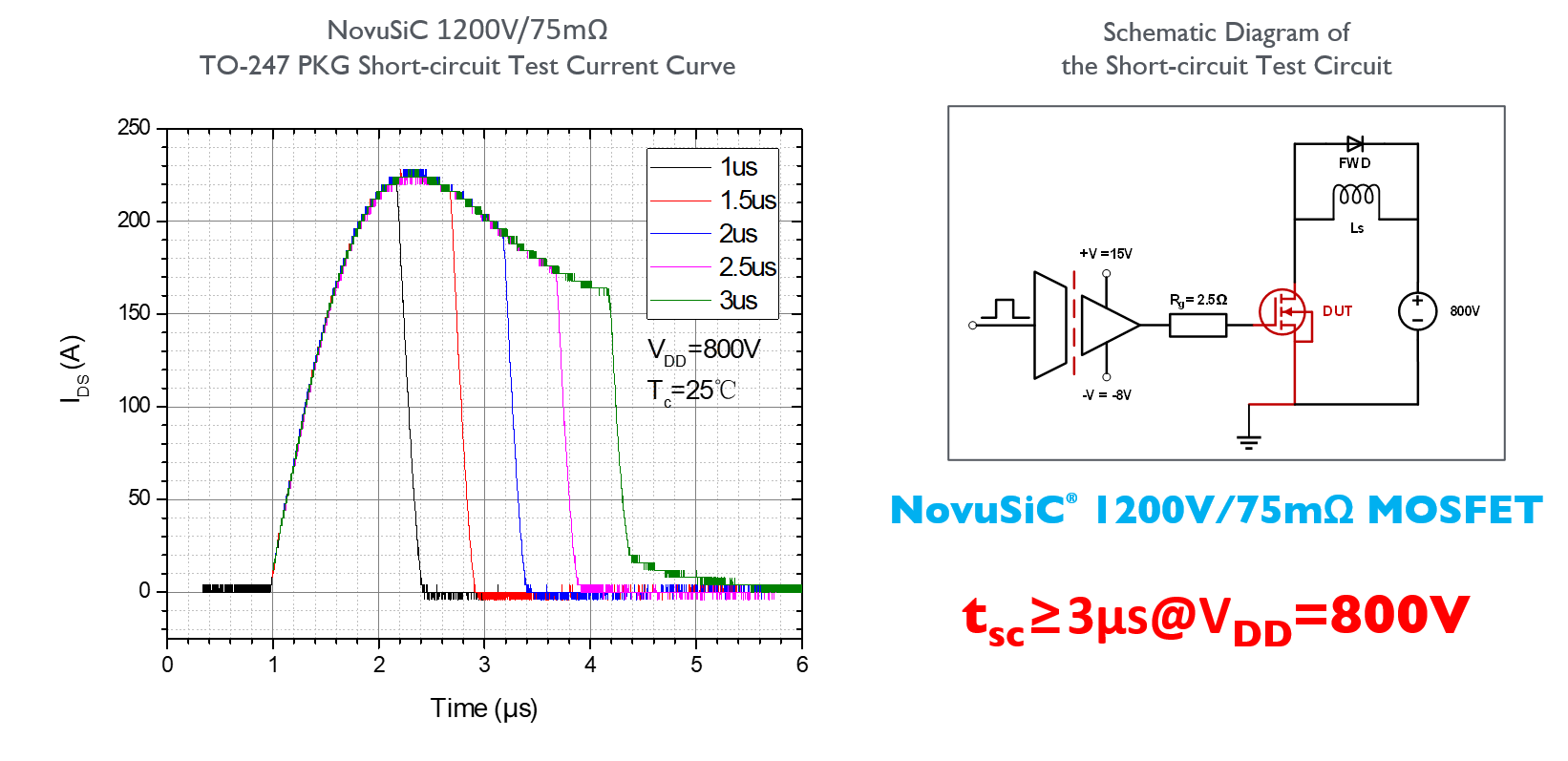
Figure 2: Short-circuit robustness of NovuSiC® 1200V/75mΩ MOSFETs
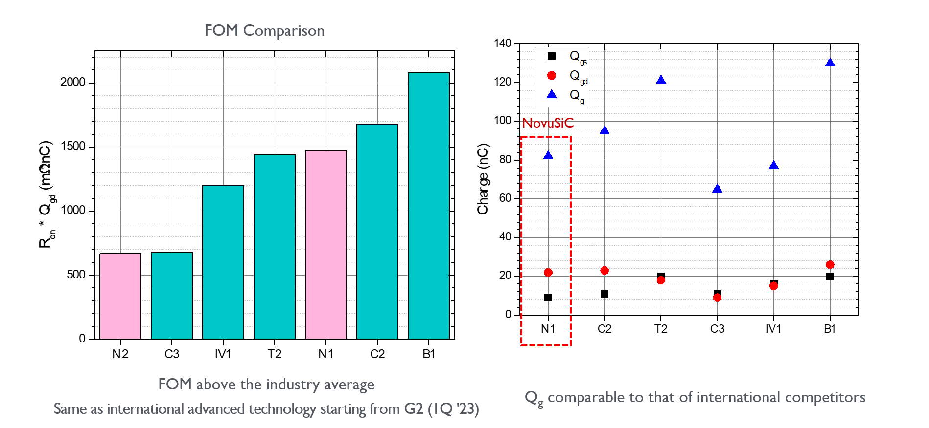
Figure 3: Comparison of Qg and FOM among different vendors
In response to risks such as FN tunneling, trap-assisted tunneling, and the degradation and failure of the gate oxide caused by external defects, Novusem proposed a targeted optimization strategy of "controlling the electric field of the gate oxide and improving the quality of the gate oxide/screening out gate oxide defects" to further improve the reliability of the gate oxide.
1. In planar SiC MOSFETs, the high electric fields of the gate oxide
are mainly concentrated in the channel and the gate oxide center in the JEFT region.
(1) For the electric fields at the channel: ensures the long-term reliability of the gate oxide by using a lower working gate voltage.
(2) For the gate oxide center in the JEFT region: designed with a lower electric field intensity at the rated blocking voltage of 1200V than the conventional limit of 4.0 MV/cm in order to reduce the electric field intensity.
2. WLTBI (Wafer-Level Test & Burn-In) is introduced in the wafer testing stage to screen out any potential degradation/failure of the gate oxide in the product life cycle.
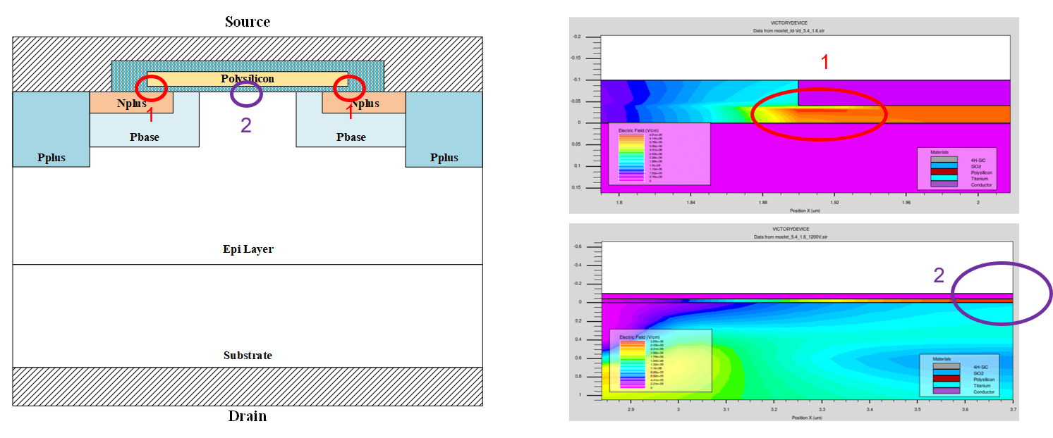
Figure 4: Novusem's reliability assurance strategy
In addition to a detailed introduction to NovuSiC® 1200V/75mΩ MOSFET G1, Dr. Gao Wei also gave a preview of the development progress and performance advantages of G2.
NovuSiC® MOSFET G2 is manufactured based on a more advanced and innovative design and process, thus significantly improving static and dynamic performance: reducing the Ron,sp by 24% and Qg by 25%. This renders the second generation of NovuSiC® MOSFETs with the performance strengths of high efficiency, high switching frequency, and high power density.
Meeting the Application Needs of New Energy Vehicles and Promoting Vehicle Electrification in China
It is a major trend to apply SiC power devices to new energy vehicles, charging piles, electric drive control systems, and other fields since they can improve vehicle efficiency and increase mileage. Given China's enormous market, there is a great demand for the industry. Novusem has launched the cost-effective NovuSiC® series and the highly-reliable DuraSiC® series for different application scenarios, among which the DuraSiC® series is mainly used in on-board chargers (OBCs) and vehicle-mounted DC-DC.
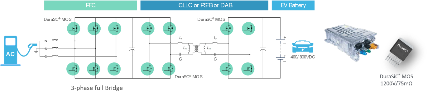
Figure 5: OBC 800V battery platform system
Currently, with the increasing demand for fast charging and bidirectional charging/discharging, the OBC input voltage has been raised to 380VAC, and the battery voltage has been raised to 800V. Using 1200V SiC devices can simplify the system topology to meet the requirements of high voltage applications. The main topology adopts the three-phase full-bridge PFC and the bidirectional resonant DC-DC topology of all-SiC MOSFETs to implement bidirectional charging and discharging. This helps increase the power to over 11 kW, lower losses by more than 50% thus increasing the peak efficiency by more than 97%, and reduce the size of magnetic devices by more than 70%.
In the field of DC charging piles, there is a clear trend of high-voltage, intelligent, and diversified development. In terms of the main topology of the DC charging module, Novusem's NovuSiC® solution provides various advantages such as a simple DC-DC system design, ease of control, low switching loss, and obvious efficiency improvements, which can help release more control resources.
In the application of 10kW PV inverters, compared to silicon-based IGBT solutions, the NovuSiC® solution can reduce the total loss by 50% and improve the efficiency by 2% at a switching frequency of 20 kHz, or it can double the switching frequency and reduce the system volume by more than 60% at the same total loss.
To help customers evaluate the feasibility of solutions in the early stages of product development, Novusem specially developed the "EVAL-MAIN" evaluation board. With this evaluation board, customers can perform single-pulse and double-pulse tests to assess the dynamic performance of switch transistors.

Figure 6: Physical picture of the NovuSiC® MOSFET driver evaluation board
This evaluation board consists of a mother board and a flexible driver daughter board and provides two isolation solutions: capacitive isolation and magnetic isolation. It is applicable to TO247-3 and TO247-4 packaged SiC MOSFETs and is compatible with various driver chips for testing and evaluation.
Epilogue
Every step Novusem has taken since inception has been steadfast and steady. The company has been realistic and earnest in every link of product development to meet demand and create value for customers. In the future, Novusem will "accumulate strength and continue innovation" to accelerate its progress towards the goal of leading power semiconductor R&D and manufacturing in China, contributing to China's journey towards "carbon peaking and carbon neutrality" through scientific and technological innovation.